Solar cells are divided into crystalline silicon and amorphous silicon, among which crystalline silicon cells can be further divided into monocrystalline cells and polycrystalline cells; the efficiency of monocrystalline silicon is different from that of crystalline silicon.
Classification:
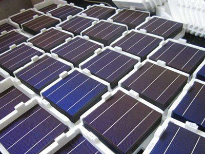
The commonly used solar crystalline silicon cells in China can be divided into:
Single crystal 125*125
Single crystal 156*156
Polycrystalline 156*156
Single crystal 150*150
Single crystal 103*103
Polycrystalline 125*125
Manufacturing process:
The production process of solar cells is divided into silicon wafer inspection – surface texturing and pickling – diffusion junction – dephosphorization silicon glass – plasma etching and pickling – anti-reflection coating – screen printing – Rapid sintering, etc. The details are as follows:
1. Silicon wafer inspection
Silicon wafers are the carriers of solar cells, and the quality of silicon wafers directly determines the conversion efficiency of solar cells. Therefore, it is necessary to inspect incoming silicon wafers. This process is mainly used for online measurement of some technical parameters of silicon wafers, these parameters mainly include wafer surface unevenness, minority carrier lifetime, resistivity, P/N type and microcracks, etc. This group of equipment is divided into automatic loading and unloading, silicon wafer transfer, system integration part and four detection modules. Among them, the photovoltaic silicon wafer detector detects the unevenness of the surface of the silicon wafer, and simultaneously detects the appearance parameters such as the size and diagonal of the silicon wafer; the micro-crack detection module is used to detect the internal micro-cracks of the silicon wafer; in addition, there are two Detection modules, one of the online test modules is mainly used to test the bulk resistivity of silicon wafers and the type of silicon wafers, and the other module is used to detect the minority carrier lifetime of silicon wafers. Before the detection of minority carrier lifetime and resistivity, it is necessary to detect the diagonal and micro-cracks of the silicon wafer, and automatically remove the damaged silicon wafer. Silicon wafer inspection equipment can automatically load and unload wafers, and can place unqualified products in a fixed position, thereby improving inspection accuracy and efficiency.
2. Surface textured
The preparation of monocrystalline silicon texture is to use the anisotropic etching of silicon to form millions of tetrahedral pyramids, that is, pyramid structures, on the surface of every square centimeter of silicon. Due to the multiple reflection and refraction of incident light on the surface, the absorption of light is increased, and the short-circuit current and conversion efficiency of the battery are improved. The anisotropic etching solution of silicon is usually a hot alkaline solution. The available alkalis are sodium hydroxide, potassium hydroxide, lithium hydroxide and ethylenediamine. Most of the suede silicon is prepared by using an inexpensive dilute solution of sodium hydroxide with a concentration of about 1%, and the etching temperature is 70-85 °C. In order to obtain a uniform suede, alcohols such as ethanol and isopropanol should also be added to the solution as complexing agents to accelerate the corrosion of silicon. Before the suede is prepared, the silicon wafer must be subjected to preliminary surface etching, and about 20-25 μm is etched with an alkaline or acidic etching solution. After the suede is etched, general chemical cleaning is performed. The surface-prepared silicon wafers should not be stored in water for a long time to prevent contamination, and should be diffused as soon as possible.
3. Diffusion knot
Solar cells need a large-area PN junction to realize the conversion of light energy to electric energy, and a diffusion furnace is a special equipment for manufacturing the PN junction of solar cells. The tubular diffusion furnace is mainly composed of four parts: the upper and lower parts of the quartz boat, the exhaust gas chamber, the furnace body part and the gas cabinet part. Diffusion generally uses phosphorus oxychloride liquid source as diffusion source. Put the P-type silicon wafer in the quartz container of the tubular diffusion furnace, and use nitrogen to bring phosphorus oxychloride into the quartz container at a high temperature of 850-900 degrees Celsius. The phosphorus oxychloride reacts with the silicon wafer to obtain phosphorus. atom. After a certain period of time, phosphorus atoms enter the surface layer of the silicon wafer from all around, and penetrate and diffuse into the silicon wafer through the gaps between the silicon atoms, forming the interface between the N-type semiconductor and the P-type semiconductor, that is, the PN junction. The PN junction produced by this method has good uniformity, the non-uniformity of sheet resistance is less than 10%, and the minority carrier lifetime can be greater than 10ms. Fabrication of PN junction is the most basic and critical process in solar cell production. Because it is the formation of the PN junction, the electrons and holes do not return to their original places after flowing, so that a current is formed, and the current is drawn out by a wire, which is direct current.
4. Dephosphorylation silicate glass
This process is used in the production process of solar cells. By chemical etching, the silicon wafer is immersed in a hydrofluoric acid solution to produce a chemical reaction to generate a soluble complex compound hexafluorosilicic acid to remove the diffusion system. A layer of phosphosilicate glass formed on the surface of the silicon wafer after the junction. During the diffusion process, POCL3 reacts with O2 to form P2O5 which is deposited on the surface of the silicon wafer. P2O5 reacts with Si to generate SiO2 and phosphorus atoms, In this way, a layer of SiO2 containing phosphorus elements is formed on the surface of the silicon wafer, which is called phosphosilicate glass. The equipment for removing phosphorous silicate glass is generally composed of the main body, cleaning tank, servo drive system, mechanical arm, electrical control system and automatic acid distribution system. The main power sources are hydrofluoric acid, nitrogen, compressed air, pure water, heat exhaust wind and waste water. Hydrofluoric acid dissolves silica because hydrofluoric acid reacts with silica to generate volatile silicon tetrafluoride gas. If the hydrofluoric acid is excessive, the silicon tetrafluoride produced by the reaction will further react with the hydrofluoric acid to form a soluble complex, hexafluorosilicic acid.
5. Plasma etching
Since during the diffusion process, even if back-to-back diffusion is adopted, phosphorus will inevitably be diffused on all surfaces including edges of the silicon wafer. Photogenerated electrons collected on the front side of the PN junction will flow along the edge area where phosphorus is diffused to the back side of the PN junction, causing a short circuit. Therefore, the doped silicon around the solar cell must be etched to remove the PN junction at the cell edge. This process is usually done using plasma etching techniques. Plasma etching is in a low pressure state, the parent molecules of the reactive gas CF4 are excited by radio frequency power to generate ionization and form plasma. Plasma is composed of charged electrons and ions. Under the impact of electrons, the gas in the reaction chamber can absorb energy and form a large number of active groups in addition to being converted into ions. The active reactive groups reach the surface of SiO2 due to diffusion or under the action of an electric field, where they react chemically with the surface of the material to be etched, and form volatile reaction products that separate from the surface of the material to be etched, and are pumped out of the cavity by the vacuum system.
6. Anti-reflection coating
The reflectivity of the polished silicon surface is 35%. In order to reduce the surface reflection and improve the conversion efficiency of the cell, it is necessary to deposit a layer of silicon nitride anti-reflection film. In industrial production, PECVD equipment is often used to prepare anti-reflection films. PECVD is plasma enhanced chemical vapor deposition. Its technical principle is to use low-temperature plasma as the energy source, the sample is placed on the cathode of the glow discharge under low pressure, the glow discharge is used to heat the sample to a predetermined temperature, and then an appropriate amount of reactive gases SiH4 and NH3 are introduced. After a series of chemical reactions and plasma reactions, a solid-state film, that is, a silicon nitride film, is formed on the surface of the sample. In general, the thickness of the film deposited by this plasma-enhanced chemical vapor deposition method is about 70 nm. Films of this thickness have optical functionality. Using the principle of thin film interference, the reflection of light can be greatly reduced, the short-circuit current and output of the battery are greatly increased, and the efficiency is also greatly improved.
7. screen printing
After the solar cell has gone through the processes of texturing, diffusion and PECVD, a PN junction has been formed, which can generate current under illumination. In order to export the generated current, it is necessary to make positive and negative electrodes on the surface of the battery. There are many ways to make electrodes, and screen printing is the most common production process for making solar cell electrodes. Screen printing is to print a predetermined pattern on the substrate by means of embossing. The equipment consists of three parts: silver-aluminum paste printing on the back of the battery, aluminum paste printing on the back of the battery, and silver-paste printing on the front of the battery. Its working principle is: use the mesh of the screen pattern to penetrate the slurry, apply a certain pressure on the slurry part of the screen with a scraper, and move towards the other end of the screen at the same time. The ink is squeezed from the mesh of the graphic portion onto the substrate by the squeegee as it moves. Due to the viscous effect of the paste, the imprint is fixed within a certain range, and the squeegee is always in linear contact with the screen printing plate and the substrate during printing, and the contact line moves with the movement of the squeegee to complete the printing stroke.
8. rapid sintering
The screen-printed silicon wafer cannot be used directly. It needs to be quickly sintered in a sintering furnace to burn off the organic resin binder, leaving almost pure silver electrodes that are closely adhered to the silicon wafer due to the action of glass. When the temperature of the silver electrode and the crystalline silicon reaches the eutectic temperature, the crystalline silicon atoms are integrated into the molten silver electrode material in a certain proportion, thereby forming the ohmic contact of the upper and lower electrodes, and improving the open circuit voltage and filling factor of the cell. The key parameter is to make it have resistance characteristics to improve the conversion efficiency of the cell.
The sintering furnace is divided into three stages: pre-sintering, sintering, and cooling. The purpose of the pre-sintering stage is to decompose and burn the polymer binder in the slurry, and the temperature rises slowly at this stage; in the sintering stage, various physical and chemical reactions are completed in the sintered body to form a resistive film structure, making it truly resistive. , the temperature reaches a peak in this stage; in the cooling and cooling stage, the glass is cooled, hardened and solidified, so that the resistive film structure is fixedly adhered to the substrate.
9. Peripherals
In the process of cell production, peripheral facilities such as power supply, power, water supply, drainage, HVAC, vacuum, and special steam are also required. Fire protection and environmental protection equipment are also particularly important to ensure safety and sustainable development. For a solar cell production line with an annual output of 50MW, the power consumption of the process and power equipment alone is about 1800KW. The amount of process pure water is about 15 tons per hour, and the water quality requirements meet the EW-1 technical standard of China’s electronic grade water GB/T11446.1-1997. The amount of process cooling water is also about 15 tons per hour, the particle size in the water quality should not be greater than 10 microns, and the water supply temperature should be 15-20 °C. The vacuum exhaust volume is about 300M3/H. At the same time, about 20 cubic meters of nitrogen storage tanks and 10 cubic meters of oxygen storage tanks are also required. Taking into account the safety factors of special gases such as silane, it is also necessary to set up a special gas room to absolutely ensure production safety. In addition, silane combustion towers and sewage treatment stations are also necessary facilities for cell production.
Post time: May-30-2022